The Semiconductor Illusion: Why the Real Billions in India’s Tech Boom Are Hidden in the Midstream
Global technology coverage has locked onto a single, high-stakes headline: India’s multi-billion-dollar push into semiconductor fabrication.
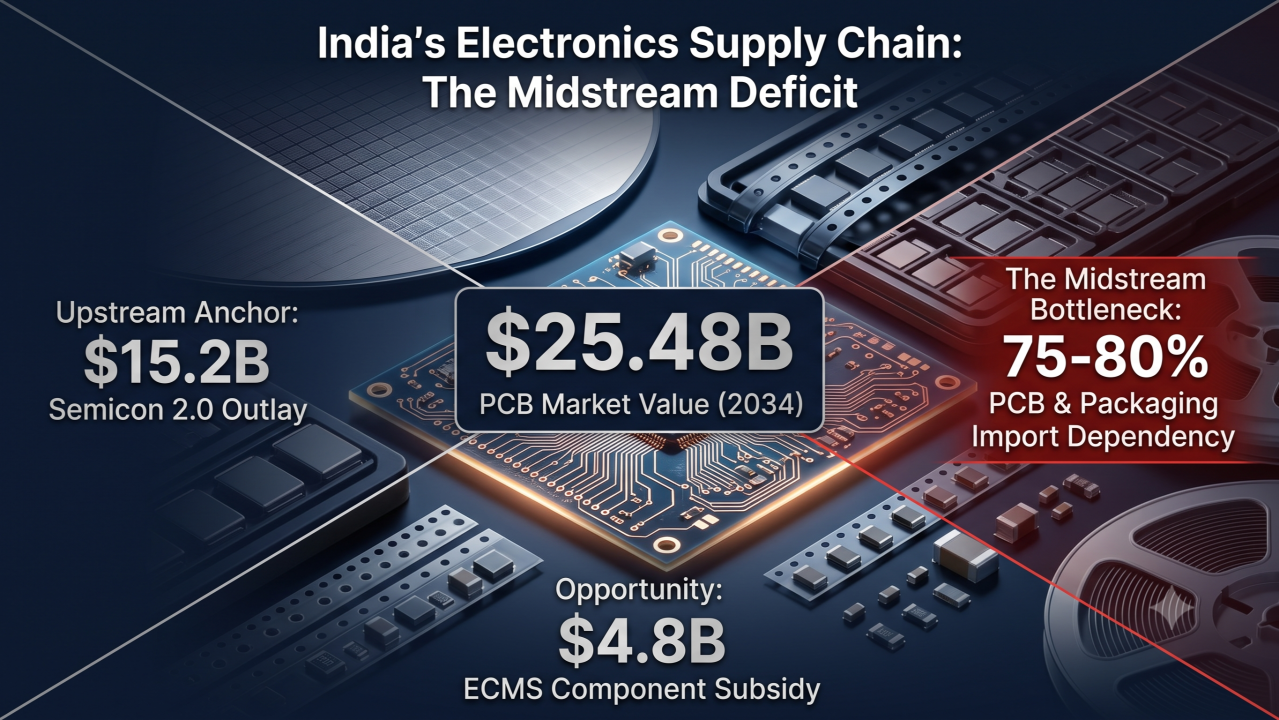
Project approvals have crossed INR1.64 lakh crore under the India Semiconductor Mission (ISM), headlined by commercial foundries aiming for 50,000 wafer starts per month in Dholera and advanced packaging hubs in Assam and Sanand engineered to output tens of millions of units daily. The recent cabinet approval of Semicon 2.0, backed by a INR1,27,500 Crore (~$14B) outlay, has cemented the country's ambition to become a global silicon heavyweight.
Yet, this obsession with front-end cleanrooms has created an industry-wide blind spot.
A raw silicon die is useless in isolation. It cannot sit on a table, plug into an engine, or compute a line of logic without an entire physical architecture built around it. Long before a processor reaches a smartphone, an automobile, or an industrial robot, it must be shielded by precision packaging media, wired onto a printed circuit board, supported by hundreds of passive components, and integrated into a final chassis.
While capital queues up behind the foundries, the real industrial bottleneck and the most accessible, high-margin commercial opportunity lies in the far less capital-intensive midstream layers.
1. The Packaging Paradox: Billions in Silicon, Reliant on Imported Plastics
The first major vulnerability appears the second a silicon wafer is diced. Bare dies require an intricate, highly specialized supporting cast of packaging consumables: high-temperature matrix trays, automated embossed carrier tapes, plastic reels, and moisture-barrier bags to survive transit and high-speed pick-and-place lines.
Despite committing tens of billions of dollars to domestic assembly lines, India remains almost entirely dependent on East Asian imports for these precision handling media.
This creates a structural margin penalty for local manufacturing. Rigid plastics cannot be compressed for shipping; importing empty trays and bulky reels means paying for international volumetric freight, port handling, compounding customs tariffs, and the working capital cost of holding months of safety buffer stock to prevent automated assembly lines from stalling.
Setting up a certified cleanroom injection molding and continuous tape extrusion facility costs a tiny fraction of a silicon fab, yet it delivers immediate operating leverage. As domestic OSATs shift from manual pilot handling to automated mass production, domestic packaging consumables represent a vital, high-margin necessity that the market is largely ignoring.
2. The PCB Deficit: An $8B to $25B Runway Strangled by Imports
Once a chip is packaged, it needs a structural foundation the Printed Circuit Board (PCB). Even before the semiconductor mission gained momentum, India’s domestic PCB ecosystem was struggling under severe import dependency.
According to market projections, India's PCB market is on track to surge from $7 Billion in 2025 to $25.48 Billion by 2034, compounding at nearly 15% annually. Yet local bare-board fabrication satisfies only 20% to 25% of current domestic demand. The remaining 75% to 80% is imported, primarily from China, Taiwan, and South Korea.
The domestic supply reality breaks down as follows:
- Domestic Output: 20% to 25% of total demand
- Foreign Imports: 75% to 80% of total demand
Worse still, what India does manufacture domestically is overwhelmingly concentrated at the low end: single-sided boards account for roughly 53% of local output. The advanced multi-layer (8 to 20+ layers), flexible circuits, and High-Density Interconnect (HDI) boards required for 5G infrastructure, electric vehicles, and smartphones are almost entirely brought in from overseas.
This creates an obvious contradiction: fabricating advanced chips locally only to export them for mounting onto foreign boards, or importing empty boards to house domestic chips, defeats the entire logic of supply-chain sovereignty.
Policy is actively pivoting to address this gap. The government expanded the Electronics Component Manufacturing Scheme (ECMS) to INR40,000 Crore, offering up to 25% capital expenditure subsidies alongside tiered turnover incentives specifically for multi-layer PCBs, HDI boards, and flexible circuits. Furthermore, targeted trade remedies are already shaping procurement; an anti-dumping duty covers lower-layer imported boards (up to 6 layers), while high-layer, flexible, and HDI boards remain duty-exempt pointing directly to where domestic technical capabilities must be built.
3. The Missing Capillaries: Passives, Substrates, and Chemicals
A complete electronics ecosystem requires far more than just silicon and bare boards:
- Passive Components (MLCCs, Resistors, Inductors): For every complex processor on a board, there are hundreds of miniature passives regulating voltage, filtering noise, and managing signal timing. The vast majority of these surface-mount devices are imported in the billions, creating another supply-chain choke point.
- Copper Clad Laminates (CCL) & Process Chemicals: Domestic board shops historically faced a 30% to 50% cost disadvantage versus East Asian mega-factories, driven by a near-total reliance on imported laminates, dry films, and precision plating chemicals.
- IC Substrates & Cleanroom Inputs: Advanced packaging demands specialized organic and ceramic substrates to bridge nanoscale silicon to macro-scale motherboards.
This reality explains why Semicon 2.0 was designed with an expanded INR1,27,500 Crore (~$14B) outlay. Unlike the initial phase, which focused heavily on securing marquee anchor plants, Semicon 2.0 directly targets the supply-chain backbone. Its dedicated "Machines and Materials" pillar funds the local production of specialty chemicals, process gases, and equipment spares, aiming to create an end-to-end ecosystem capable of supporting an anticipated $200 Billion domestic electronics market by 2035.
4. Supply Chain Geometry: Why Component Makers Follow EMS, Not Fabs
A common strategic mistake among potential investors is assuming that PCB fabricators and component suppliers must set up shop directly next to silicon foundries.
Operational reality works differently: component fabricators do not follow foundries; they follow downstream Electronics Manufacturing Services (EMS) and box-build assembly lines.
Assembly giants like Dixon, Foxconn, and Flex already producing over 1.2 billion mobile devices annually in India require Just-In-Time (JIT) component delivery to manage working capital and cut lead times by 30% to 40%.
This dynamic is establishing distinct, specialized regional hubs across India:
- The Western Corridor (Sanand & Dholera, Gujarat): The primary center for high-density semiconductor assembly and wafer fabrication.
- The Northern Corridor (Noida & Greater Noida, Uttar Pradesh): The consumer electronics and display powerhouse, anchoring massive handset EMS lines and display-driver assembly projects near the Yamuna Expressway.
- The Southern & Eastern Clusters: Specialized regional hubs in Tamil Nadu, Karnataka, and Assam handling system integration and high-density packaging.
5. The Fast-Track Playbook: Bypassing Regulatory Red Tape
For international component suppliers evaluating the Indian market, direct cross-border equity investments and majority Joint Ventures (JVs) often face extended regulatory screening under Press Note 3 (PN3).
However, market access can be achieved far faster through asset-light, non-equity operational routes:
- Technology Licensing & Know-How Agreements: Partnering with Indian industrial groups building greenfield plants under the INR40,000 Crore ECMS scheme. International firms license their CAM engineering workflows, multi-layer routing protocols, and quality systems in exchange for recurring royalties and long-term material supply contracts.
- Bonded Warehousing in Free Trade Warehousing Zones (FTWZ): Shipping bulk inventory duty-free into bonded FTWZ hubs in Gujarat or Chennai. Domestic EMS buyers draw down boards and components on a line-side JIT basis, clearing customs only upon physical consumption.
- Contract Manufacturing Alliances: Retaining high-end HDI prototyping and ultra-high-layer production offshore while routing high-volume commercial runs through partnered domestic facilities holding local compliance badges.
The Midstream Arbitrage
Building a greenfield semiconductor fab requires billions of dollars, immense cleanroom footprints, and years of yield stabilization. In contrast, the midstream infrastructure precision packaging lines, multi-layer PCB shops, and passive component manufacturing demands a fraction of the capital while benefiting from the exact same policy wave and structural tailwinds.
The silicon heart is arriving. But the real, sustainable wealth of India’s electronics revolution will be captured by the companies that build the midstream ecosystem that brings that silicon to life.